Products
Contact Us
- Contact Person : Ms. Wu Joy
- Company Name : Shenzhen POE Precision Technology Co., Ltd.
- Tel : 86-755-25312250
- Fax : 86-755-25312247
- Address : Guangdong,shenzhen,POE 186 industrial Building, Hao Si Industrial Estate, Fuyong, Baoan district SZ 518008 CHINA.
- Country/Region : China
- Zip : 518034
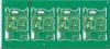
Multilayer Electronics PCB Fabric


Product Detailed
Related Categories:Multilayer PCB
Related Product Searches:Multilayer Electronics PCB Fabric,High Quality pcb fabric,pcb fabric PCB-1187
1.High quality pcb fabric
2.China professional pcb fabric manufacturer
3.POE provides pcb oem design and make services
Detailed Product DescriptionRelated Product Searches:Multilayer Electronics PCB Fabric,High Quality pcb fabric,pcb fabric PCB-1187
1.Competitive price and fast delivery2.4 Layer HASL leadfree PCB fabric manufacturing
3.ICT function and testing instruction test
4.UL certified 94v-0 pcb board
Layer: 4Layer
Material: FR4
Thickness: 1.6mm
Copper thickness: 1oz
Mini Hole: 0.2mm
Mini Width/space: 0.2mm/0.2mm
Testing points:4000
Solder Mask: LPI Green
Sickscreen: White
Function: Electronics
Finish:HASL
WELCOME TO POE
1.PCB Manufacture Capability
…………… …………… ………………
2.Leadtime for bare PCB
Production line
PCB&PCBA